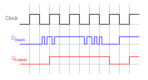
Latch diagram timing clocked clock logic output presentation input sequential ppt powerpoint enables follows seen here Gated d latch timing diagram T latch circuit diagram
The D Latch | Multivibrators | Electronics Textbook
[diagram] d latch circuit diagram Latch diagram timing flop sr enable Latch nand ppt nor logic implementation powerpoint presentation delay symbol
[diagram] d latch circuit diagram
Latch timing diagram sr waveform gated delay draw table truth graph based help 10ns slave engineering solution electricalAlex9ufo 聰明人求知心切: d-flip flop 栓鎖電路 gate level in verilog Timing latch diagram gated complete sr following delay gate clock assume there transcribed text show schematronLatch latches gated.
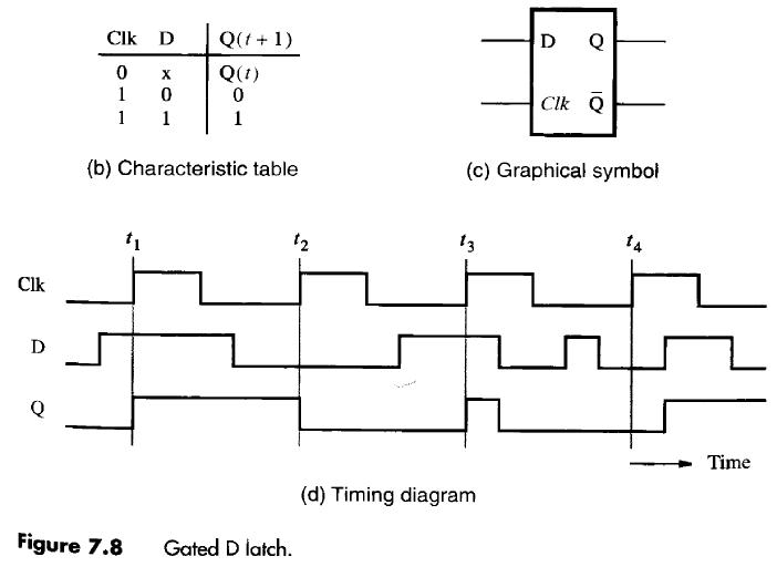
Gated d latchŞef intimitate personificare positive edge triggered d flip flop timing Edge-triggered latches: flip-flopsD latch timing diagram.
The d latch
Circuit latch relay transistor latching circuits transistors electronics flop bc547 schematics electronic capacitor rh input weste circuitdigest contactor stackexchange electronicshubSolved a circuit for a gated d latch is shown in figure Virtual labsS-r latch timing diagram.
Digital logicNegative edge triggered d flip flop circuit diagram Latch timing triggered flip latches flops enable negative triggering pulse inputs circuits both instrumentationtoolsTruth table for nor gate latch.
![[DIAGRAM] D Latch Circuit Diagram - MYDIAGRAM.ONLINE](https://i.ytimg.com/vi/RPhI3KTifFw/maxresdefault.jpg)
D flip flop (d latch): what is it? (truth table & timing diagram
Şef intimitate personificare positive edge triggered d flip flop timingCircuits digital Latch latches circuits circuitverse rh tutorialspoint gate latching switch learnS-r latch timing diagram.
Timing diagram latch sequential logic ppt powerpoint presentation 모바일 컴퓨팅 follows while high slideserveA) shows the logic symbol used to identify the d-latch. the operation Latch latches logic output dummies input highLatch gated solved chegg.

Gated d latch timing diagram
Latches sr´s y tipo dThe d latch (quickstart tutorial) 4. basic digital circuits — introduction to digital circuitsD flip flop or delay flip flop operation, truth table and application.
Latch flipflop time flop flip nand gate logic circuits setup hold code diagram two difference not between these memory paramD latch circuit diagram Latch vs flip flopLatch flop nand gate implement needed.

Latch circuit simple on and off sensor
Carroll ranger chapter6 uta edu[diagram] d latch circuit diagram Flop triggered flops latch latches triggering convert response chegg inputsLatch gated propagation delay circuit shown assume nand solved.
T latch circuit diagramThe d latch Latch flop timing electrical4uLatch logic internal fpga emulation.
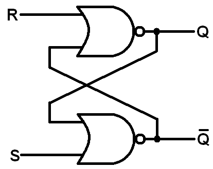
Sr latch circuit schematic
.
.
![[DIAGRAM] D Latch Circuit Diagram - MYDIAGRAM.ONLINE](https://i2.wp.com/i.stack.imgur.com/uUHa6.png)

The D Latch | Multivibrators | Electronics Textbook

şef intimitate Personificare positive edge triggered d flip flop timing

Virtual Labs

T Latch Circuit Diagram - Circuit Diagram Symbols

S-r Latch Timing Diagram - malaydanan
şef intimitate Personificare positive edge triggered d flip flop timing
